In this continuation of the tinyAVR tutorial series, this blog post delves into the AVR CPU architecture, capabilities, and registers.
Table of Contents
Features
- 8-Bit, High-Performance AVR RISC CPU:
- 135 instructions
- Hardware multiplier
- 32 8-Bit Registers Directly Connected to the Arithmetic Logic Unit (ALU)
- Stack in RAM
- Stack Pointer Accessible in I/O Memory Space
- Direct Addressing of up to 64 KB of Unified Memory:
- Entire Flash accessible with all LD/ST instructions
- True 16-Bit Access to 16-Bit I/O Registers
- Efficient Support for 8-, 16-, and 32-Bit Arithmetic
- Configuration Change Protection for System Critical Features
Overview
AVR is a well known 8-bit CPU. The CPU is a heart of the device which can access memories, do calculations, execute instructions, control peripherals as well handle interrupt routines. Most part of this post is based on the official Attiny404 documentation, so for in-depth info check the datasheet.
Architecture
AVR CPU uses a Harvard architecture with separate buses for program and data. While one instruction is being executed by the CPU, the second is being fetched from the program memory – this pipeline allows instructions to be executed on each clock cycle.
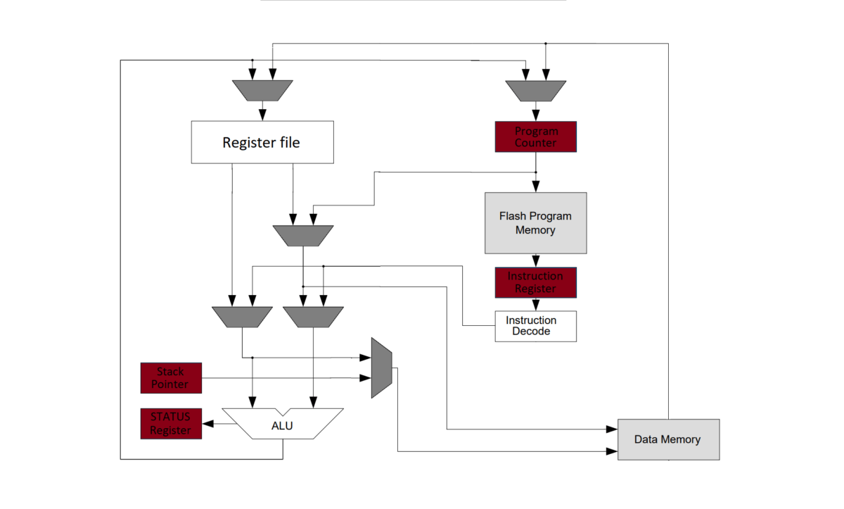
As you can see in the image above, the CPU has ALU – Arithmetic Logic Unit. It can do logic and/or arithmetic operations between two registers or a constant value and a register. Also, ALU can execute single-register operations. When the ALU finishes an arithmetic operation, the STATUS register gets updated with the information about the operation end result.
The ALU can directly access to a register file which consists of 32 8-bit general purpose working registers. All these registers have single clock cycle access time. To sum up, this allows single cycle arithmetic operations between two registers.
Memory overview
The program memory bus is directly connected to Flash, the addresses start from 0x0000. Whole data memory space is divided into I/O registers, SRAM, EEPROM and Flash.
I/O memory space, which includes all I/O Control and Status registers, takes up lowest 4KB of the data memory addresses. These can be accessed with single cycle read/write instructions, while the extended memory space IO registers (0x0040 to 0x0FFF) must be accessed as data space locations using load and store instructions.
The memory reserved for the NVM controller, EEPROM and fuses takes up address space from 0x1000 till 0x1800. The space between 0x1800 till 0x7FFF is reserved from other memories like SRAM.
The Flash starts from the 0x8000 address.
Hardware multiplier
It allows to multiply two 8-bit numbers into a 16-bit result. Different variantions of unsisghed and/or signed numbers can be used:
- Multiplication of signed/unsigned integers
- Multiplication of signed/unsigned fractional numbers
- Multiplication of a signed integer with an unsigned integer
- Multiplication of a signed fractional number with an unsigned one
A multiplication of 8-bit values takes two CPU clock cycles. It should be noted, that multiplication of higher bit values (like 16 or 32 bit) will take significantly more time.
Program flow
When the CPU is restarted, it will start executing instructions from the lowest Flash program memory address.
Most AVR instructions use a 16-bit word format, and a limited number use a 32-bit format.
When an interrupt happens, the return address is stored on the stack as a pointer. After interrupt routine, the CPU returns to the instruction which was interrupted.
Status register
After most recent arithmetic or logic operation the CPU.SREG (status register) will contain the result information. This info could be used in user program to make conditional operations.
CPU.SREG is updated after all ALU operations. CPU.SREG is not automatically saved and restored before entering or after returning from an interrupt routine. So, user code needs to take care of maintaining status register between context switches.
Stack and its pointer
Return addresses which are used after interrupt and subroutine calls are kept in the stack. The Stack Pointer (SP) always points to the top of the stack.
Data is pushed and popped from the stack using the PUSH and POP instructions. The stack grows from higher to lower memory addresses. After reset, the Stack Pointer is set to the highest location of the internal SRAM.
Register file
This file has in total of 32 8-bit registers with single clock access time.
The following I/O schemes are supported:
• One 8-bit output operand and one 8-bit result input
• Two 8-bit output operands and one 8-bit result input
• Two 8-bit output operands and one 16-bit result input
• One 16-bit output operand and one 16-bit result input
Six of the 32 registers can be used as three 16-bit Address Register Pointers for data space addressing, allowing efficient address calculations.
Access to 16-bit registers
The AVR MCU data bus is 8 bit wide, so accessing 16 bit registers use atomic operations. These registers accessed by two read and write operations.
For a write operation, the low byte of the 16-bit register must be written before the high byte. For a read operation, the low byte of the 16-bit register must be read before the high byte.
It is possible that interrupts will corrupt the sequence if an interrupt is triggered and accesses the same 16-bit register during an atomic 16-bit operation. It is best to disable interrupts when writing or reading 16-bit registers.
Configuration Change Protection (CCP)
Important, system critical registers are write-protected from accidental modification. Also, self-programming is protected from accidental execution. This (un)protection is handled by Configuration Change Protection (CCP) register.
Writing to protected register is possible after writing correct value into CCP register.
There are two working modes, hence two values, of operation: unprotecting IO registers or unprotecting self-programming.
To unlock write protected register you will need to:
- Write correct value (0xD8) into CPU.CCP register.
- Within four instructions write a value to the protected register.
To execute self-programming, you will need to:
- Write correct value (0x9D) into CPU.CCP register.
- Within four instructions, the software must execute the appropriate instruction.
Register summary
| Name | Description |
| CCP | Configuration Change Protection. Writing correct value to this register unlocks write protected registers or allows self programming. Value 0x9D is used for unlocking self-programming, while a value 0xD8 – unprotects registers. |
| SP | The CPU.SP holds the Stack Pointer (SP) that points to the top of the stack. |
| SREG | The Status register contains information about the result of the most recently executed arithmetic or logic instruction. Each bit has different meaning – chek it in the datasheet. |
Real CCP example
There’s is much to show about CPU, so let’s see a simple, yet useful example on how to write into write protected register.
CPU_CCP = 0xD8; //enable write to protected register;
CLKCTRL_MCLKCTRLB = 0; // No prescaling to periphery;
The code above unclocks write-protected register by writing 0xD8 value into CPU_CCP register. In the example, the write-protected register is CLKCTRL_MCLKCTRLB which is used to set a clock devider for periphery. So, by writing 0 to it, the periphery (like a timer) will run at CPU speed without prescaling (which in my case is 20 MHz).
Summary
To sum up, this was a short, but I hope useful intro into AVR CPU and its registers. The shown code example will let you easily modify protected control registers on the MCU.